We’re better than simply compliant.
We’re audit-ready.
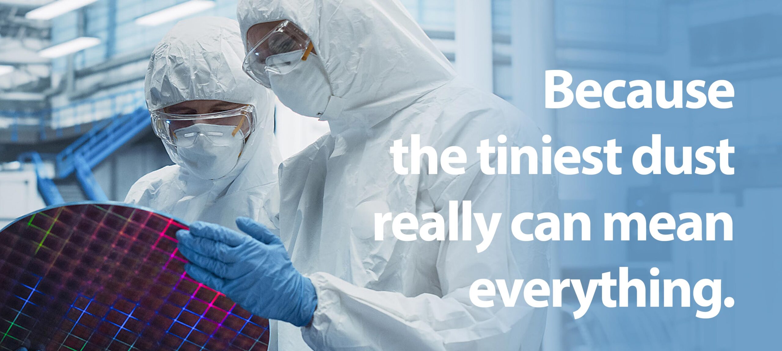
High-stakes manufacturing offers no second chances when it comes to safety or standards.
Technical precision requires a partner who deeply understands cleanroom science.
Your cleanrooms need to be sterile, be compliant, and be efficient.
You need a partner that understands the science of your space and delivers precision time after time.
Semiconductor Contamination Control
Our mission is to maximize your semiconductor wafer starts and operational uptime through uncompromising contamination control. We specialize in ISO Class 1–5 standards and AMC thresholds for submicron manufacturing, tailoring our protocols to your specific process flow and facility requirements.
Your yield targets drive our solutions—from mitigating “killer defects” through rigorous particulate management to ensuring ESD safety and documentation accuracy. Through specialized training and strict laminar flow discipline, we protect your nanoscale integrity and your bottom line.
OPTIONS INCLUDE:
SEMICONDUCTOR CLEANROOMS
PHARMACEUTICAL CLEANROOMS
BIOTECH LABORATORIES
MEDICAL DEVICE MANUFACTURING
ISO-CERTIFIED ENVIRONMENTS
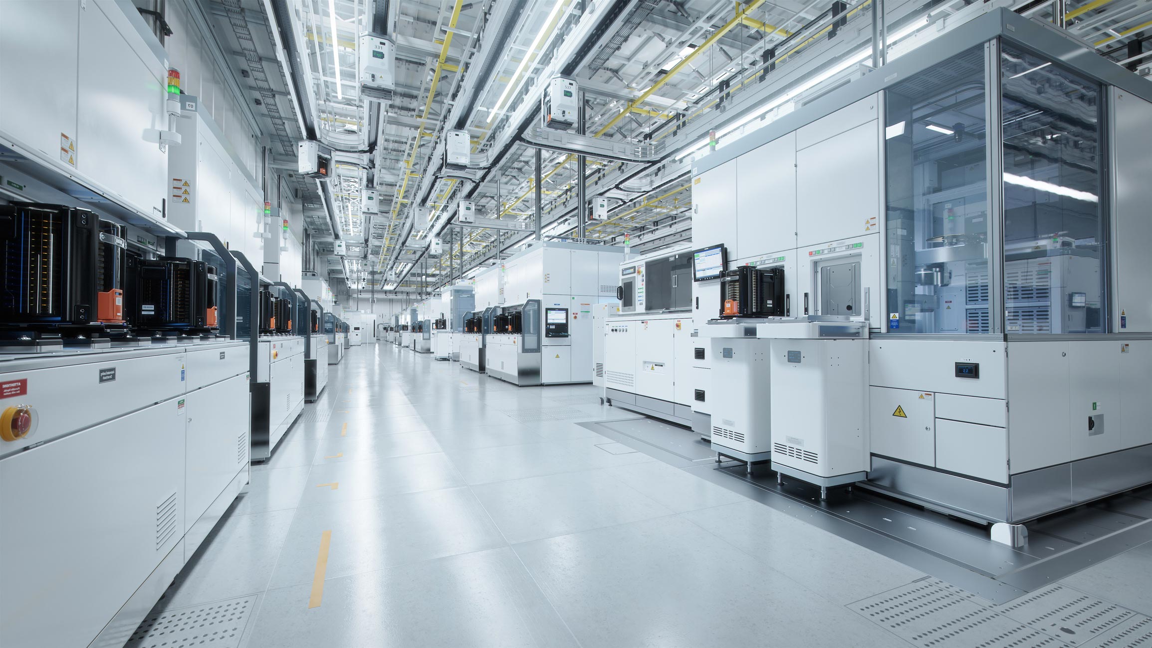
Contamination Control for Foundries, OSATs, and Sub-Micron Fab Environments
Front-end and back-end semiconductor facilities must maintain rigorous ISO Class 1–5 standards to prevent “killer defects” and maximize wafer yields. We support these high-stakes environments with specialized teams and protocols designed to mitigate Airborne Molecular Contamination (AMC), ensuring your lithography optics and vacuum systems remain uncompromised.
Specialized Fab Teams Trained for Yield Integrity
Precision Protocols. Zero “Killer Defects.” Maximum Uptime.
Sub-micron performance starts long before the first wafer enters the FOUP. It begins with technicians who understand the physics of laminar airflow, the volatility of ESD (Electrostatic Discharge), and the catastrophic impact of a single metallic particle on a 3nm gate.
Our semiconductor-specific teams undergo hands-on, ongoing training tailored to your specific process flow—from FEOL (Front-End-of-Line) chemical bays to automated assembly lines. We provide the expertise needed to prevent tool-side contamination, avoid vibration-induced recalibrations, and keep your wafer starts moving. Every service is guided by your SOPs and supported by high-purity protocols that safeguard your nanoscale integrity from the sub-floor to the ceiling plenum.
Engineering Your Semiconductor Contamination Strategy
Three steps to sub-micron precision, yield protection, and maximum uptime.
Step One: Technical Consultation
Connect with a semiconductor contamination specialist to audit your ISO Class 1–5 requirements, Airborne Molecular Contamination (AMC) thresholds, and specific lithography or etch bay constraints. We align our approach with your specific technology node and substrate sensitivity.
Step Two: Tool-Side Facility Assessment
Schedule a site walk-through to develop a customized contamination control plan. We analyze your FOUP-handling protocols, Automated Material Handling Systems (AMHS), and airflow dynamics to ensure our presence never interferes with your “Lights-Out” automation.
Step Three: Precision Yield Implementation
Deploy a data-driven protocol designed to mitigate killer defects and electrostatic discharge (ESD). Our strategy keeps your facility audit-ready and your wafer starts moving, ensuring that your nanoscale integrity remains uncompromised.
Sub-Micron Contamination Control: Maximizing Yield and Uptime
Because in semiconductor fabrication, a single “killer defect” can compromise an entire wafer.
In a high-stakes Front-End-of-Line (FEOL) environment, every nanometer matters. We keep your bays ISO Class 1-ready, your lithography optics protected, and your automated material handling systems (AMHS) moving without particulate interference.
Our technicians are rigorously trained in laminar flow discipline and ESD protocols, following site-specific SOPs with zero margin for error. The result: stabilized Airborne Molecular Contamination (AMC) levels, optimized wafer yields, and total confidence in your facility’s nanoscale integrity.
CERTIFICATIONS:

![]()

Fab Contamination Control: FAQs
How is your semiconductor cleanroom cleaning specialized?
We tailor our services to the rigorous demands of sub-micron manufacturing. Our teams are trained specifically in ISO Class 1–5 protocols, focusing on Airborne Molecular Contamination (AMC) and particulate control. The result is a stable environment that protects your wafer yield and lithography optics.
How do you prevent contamination during the cleaning process?
Technicians follow strict laminar flow discipline, using specialized vacuum systems and ultra-low-linting materials that align with your ISO classification. Every movement is engineered to avoid airflow disruption or the introduction of “killer defects.” We clean with surgical precision to maintain uptime, not interrupt it.
What is included in a typical fab cleaning scope?
Each program is customized to your facility’s layout, typically including plenum cleaning, sub-floor decontamination, FOUP-compatible surface wipes, and ionizing grid maintenance. We also provide specialized micro-cleaning for tool-side support and high-purity chemical area sanitation.
How do you support documentation and protocol compliance?
We adhere to strict Standard Operating Procedures (SOPs) to ensure every task is traceable. Technicians log timestamps, area-specific particle counts (if required), and material batches used. You receive complete, audit-ready records that integrate with your facility’s Quality Management System.
Can you assist with cleanroom certification or “Lights-Out” readiness?
Yes. We support pre-certification deep cleans, protocol audits, and readiness checks for automated material handling environments. We understand the high-stakes pressure of a fab ramp-up and ensure your environment meets sub-nanometer requirements without stressing your internal engineering team.
What specialized training do your technicians receive?
Our team undergoes rigorous onboarding in:
-
ESD (Electrostatic Discharge) prevention
-
ISO 14644 standards and particle physics
-
Advanced cleanroom gowning and “Air-Shower” etiquette
-
Tool-side safety and vacuum protocols
-
Traceable documentation accuracy
Do you serve facilities outside of silicon wafer fabrication?
Absolutely. We support the entire microelectronics ecosystem, including MEMS, LED, solar cell manufacturing, and high-vacuum research labs where sub-micron cleanliness is a non-negotiable requirement.
Want to learn more? Contact us today.